





 Saturday, 24-10-26








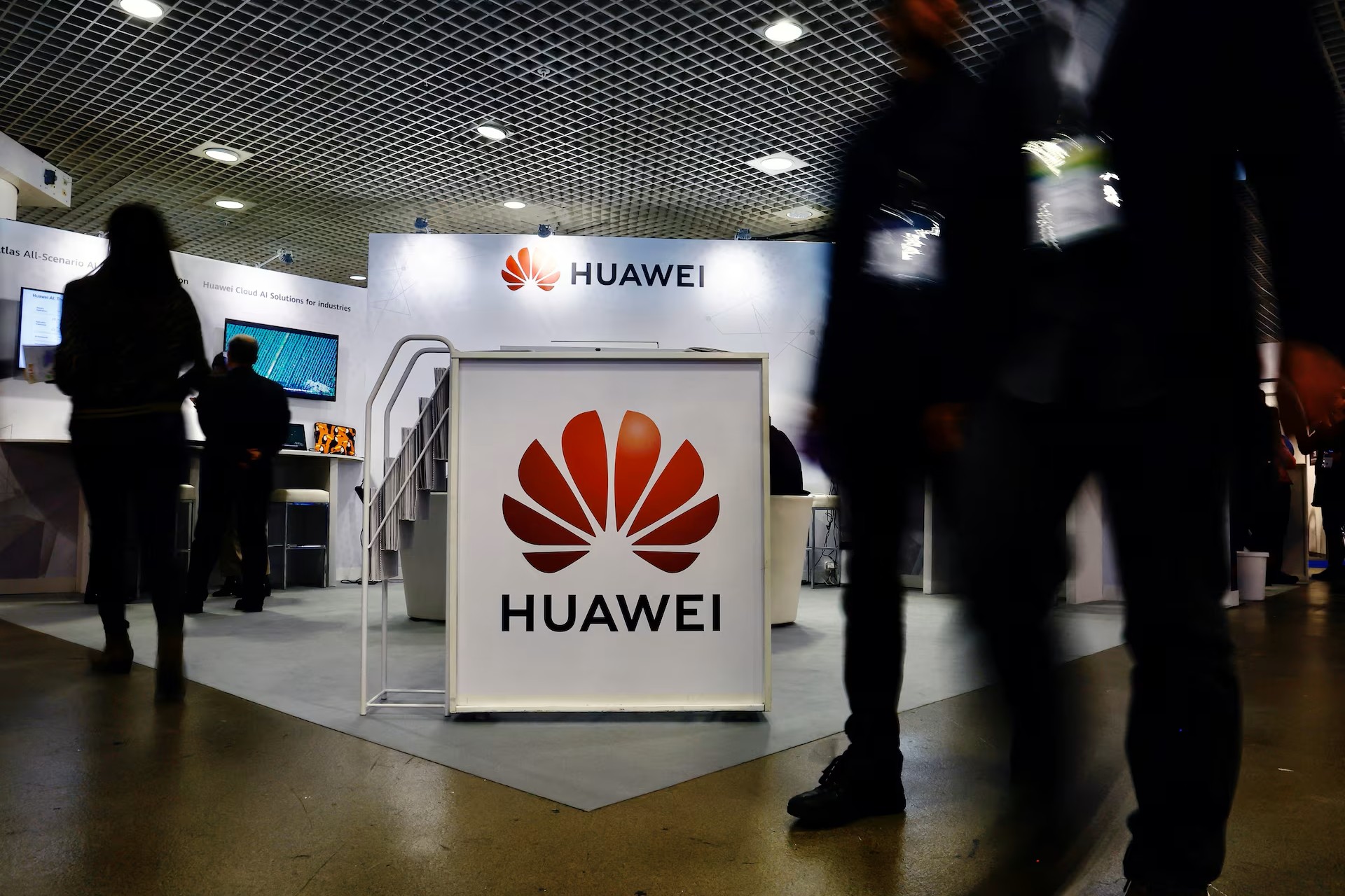
Huawei Technologies has introduced a new semiconductor efficiency framework called the Tau Scaling Law, marking a strategic shift in chip development.
The approach focuses on improving performance by reducing the distance that data travels within a processor rather than relying on smaller transistors. The concept was outlined by Huawei’s semiconductor chief, He Tingbo.
This development comes as global technology firms such as Amazon, Meta Platforms, and Microsoft continue investing heavily in AI infrastructure and advanced computing systems.
At the same time, China faces limitations in accessing cutting-edge semiconductor manufacturing tools due to US export restrictions.
LogicFolding Concept Challenges Traditional Moore’s Law Approach
The Tau Scaling Law departs from the long-standing industry principle known as Moore’s Law, which emphasizes doubling transistor density to enhance performance.
Instead, Huawei proposes a method called LogicFolding. This involves dividing chip layouts into stacked computing layers, allowing data to move more quickly within the processor.
Unlike traditional flat chip designs, this vertical architecture aims to improve efficiency through structural redesign rather than transistor miniaturization.
Huawei argues that this shift is necessary as the industry reaches physical limits in shrinking chip components.
The company is currently constrained to producing chips at around a 7-nanometre scale due to restricted access to advanced manufacturing tools, including extreme ultraviolet lithography systems.
Market Rally Driven by Huawei and SMIC Investor Optimism
Huawei’s announcement triggered strong investor interest across China’s semiconductor sector.
Shares of its manufacturing partner Semiconductor Manufacturing International Corporation (SMIC) rose nearly 6 per cent following the news.
Investors are betting that Huawei’s design innovation could help Chinese chipmakers reduce dependence on foreign technology while improving competitiveness in AI-driven computing markets.
The optimism reflects broader expectations that domestic firms can adapt under ongoing US trade restrictions.
Engineering Limits and Commercial Challenges Ahead
Despite the optimism, the LogicFolding approach faces significant technical barriers.
Stacking chip layers increases manufacturing complexity and raises the risk of production defects, which could reduce yield rates.
Thermal management is another major concern, as denser chip structures may trap heat and require more advanced cooling solutions.
The concept is not entirely new, as firms such as Taiwan Semiconductor Manufacturing Company (TSMC) already use advanced chip stacking technologies, but Huawei’s approach is more aggressive in architectural redesign.
Huawei has indicated plans to deploy its first LogicFolding-based chips in smartphones later this year, with long-term goals of achieving performance comparable to 1.4-nanometre chips by 2031.
PHOTO: REUTERS/ERIC GAILLARD
This article was created with AI assistance.
We make every effort to ensure the accuracy of our content, some information may be incorrect or outdated. Please let us know of any corrections at [email protected].
Read More